Instantiate AXI VDMA IP for 1 frame, S2MM only, no SG mode
Even though the "Ubuntu on Zedboard" reference HW design I have been using already has an axi_vmda instance (see writeup of what I learned from the reference design below), I choose to create a new AXI VDMA IP core, to isolate changes from existing WORKING HW.
In Vivado block diagram view, click the "Add IP" icon on the left toolbar --> type "vdma" --> choose the only IP that shows up. Move that IP to right above the axi_hdmi_dma instance (again, discussed below) and rename it to img_vdma. Double click on the img_vdma instance to configure it as follows:
- Disable read channel altogether
- Reduce frame buffers to 1. The frame count is reduced at the end of a successful frame transfer. When this count reaches down to 0, an interrupt will be raised. 1 frame buffer disables the more advanced (but unnecessary for my application) features like scatter-gather, and genlock. Scatter-gather feature might be important for multi-ROI (region of interest) image. But the sensor I am bringing up only supports 1 ROI, so I can safely ignore SG scenario altogether and sequentially capture an image and then DMA the read out image (single ROI) to the DRAM. It makes the 1st take of the code simple AND useful!
- I set the memory map width is 64 bits, but in auto mode, Vivado changed it to 32 bits?!
- Line buffer depth is 512; is this in bytes or transactions?
- I tried to reduce the stream data width from 32 bits to 16, but the Wizard has grayed out that choice.
- In advanced tab, I turned off Fsync option, to keep things simple.
The resulting IP, with the S_AXI_S2MM port expanded for better discourse, is yet unconnected to other IPs, as shown below:
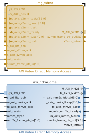
Taking care of the simple connections first, AXILite clock is connected to the FCLK_CLK0 (running at 100 MHz) from PS7, just as for the axi_hdmi_dma. Similarly, axi_resetn is connected to the system reset logic sys_rstgen's peripheral_aresetn[0], also just as for the axi_hdmi_dma. s2mm_frame_ptr_out and s2mm_frame_ptr_in are left unconnected because I do NOT use the genlock feature. m_axi_s2mm_aclk is the memory interface clock, and should be the same source as axi_hdmi_dma's m_axis_mm2s_aclk, which is FCLK_CLK0.
AXI Lite interface
The IP is controlled through memory mapped registers exposed to the M_AXI_GP0 (general purpose AXI master interface 0) port on PS7. axi_hdmi_dma connects to the master port M03_AXI in axi_cpu_interconnect, whose 7 master ports are fully taken. So I added another master port to axi_cpu_interconnect, and connected the new master port to S_AXI_LITE port. The Vivado address editor then shows the AXILite slave (img_vdma) as unconfigured, indicating that the register base address needs to be assigned to the new AXILite slave. I right clicked on the img_vmda instance in the "Address Editor" --> Auto assign address, and was assigned 0x43010000, as shown here:

High performance AXI interface to the new VDMA IP
Similar to the axi_hdmi_dma's connection to the PS7's S_AXI_HP0 (see more detailed discussion below), I added S_AXI_HP1 to PS7, at 64-bit data width.
 The PS7 customization wizard --> PS-PL Configuration tab --> HP slave AXI interface --> S_AXI_HP1 interface --> S_AXI_HP1_DATA_WIDTH offers 32 bit option, but apparently this does NOT work with the Zynq DDR controller--I lost every other word the img stream generator sent when I tried this option.
I cannot connect the PS7's HP1 directly to img_vdma's M_AXI_S2MM port; I have to go through an interconnect, as in the axi_hdmi_dma case, to translate between AXI4 and AXI3--which the interconnect does internally. This will leave the S2MM port of img_vdma instance looking for a base address on the PS7, as shown in the screenshot of the Address Editor tab below:
I cannot connect the PS7's HP1 directly to img_vdma's M_AXI_S2MM port; I have to go through an interconnect, as in the axi_hdmi_dma case, to translate between AXI4 and AXI3--which the interconnect does internally. This will leave the S2MM port of img_vdma instance looking for a base address on the PS7, as shown in the screenshot of the Address Editor tab below:

Right clicking on sys_ps7 --> Assign Address will resolve the offset and range, and make the interface appear similar to S_AXI_HP0.
Connecting the vmda interrupt to the CPU
The PS currently has 4 interrupt pins allocated for the FPGA --> PS direction; Zynq apparently allows up to 16 such interrupt pins, as you can see in the screenshot of the PS7 config wizard Interrupts tab view below.

Resuming, if I connect the img_vdma's s2mm_introut to sys_concat_intc's "In 1" port above, I can expect the SW notion of the interrupt number will be 56 + 32 = 88, which in the shared peripheral interrupt range.
Interconnect between AXI VDMA and my custom video logic--as seen on the AXI VDMA side
So far, the VDMA connection was a generic affair: not much application specific part. The S_AXIS_S2MM is the completely application specific portion of the Xilinx VDMA design, consisting of these pins:
- input s_axis_s2mm_tdata[31:0]
- input s_axis_s2mm_tkeep[3:0]: for each byte of the data, indicates which byte is valid. For most use cases, all bytes are valid. For my custom application, I will always generate 2 16-bit pixels at a time, so tkeep[3:0] should be 4'b1111.
- input s_axis_s2mm_tlast: indicates the last burst of pixels from the frame generator.
- output s_axis_s2mm_tready: VDMA deasserts this pin if it cannot receive data. The frame source should throttle output using a BRAM FIFO with sufficient headroom.
- input s_axis_s2mm_tuser[0:0]: indicates start of frame, but irrelevant for how I configured VDMA, since I turned off frame sync feature in the IP configurator.
- input s_axis_s2mm_tvalid: assert only when the tdata is valid. So for example, should probably be 0 during horizontal blank period.
- input s_axis_s2mm_aclk: this is actually NOT grouped under S_AXIS_S2MM bus, but nonetheless logically tied to the data bus coming from the custom logic.
Now I need a custom IP that will generate these signals.
A dummy IP to create the frame data
To test the VDMA, I create a new IP block that will effectively host the M_AXIS_S2MM interface (only logically, because it is NOT possible to group these S_AXIS_S2MM pins into an interface, even though Vivado has a concept of interfaces, as explained in the Xilinx document UG994: Vivado IP Subsystems. Others have tried, and Xilinx has advised against creating a user defined interface. I first thought that since Vivado already knows about S_AXIS_S2MM interface, I can just use it in my IP, but what I actually need is M_AXIS_S2MM--that is, opposite gender--which does NOT exist in /opt/Xilinx/Vivado/2014.4/data/ip/xilinx folder).
Now I have to create an IP that I will later add to the top level system block (system.bd; which contains all other system blocks), for which this blog entry is a good tutorial. But before I can create a new peripheral, I have work around a Vivado bug, as described in this Xilinx AR. In the Tools --> Project Settings --> IP --> Packager --> IP location, set the IP location to ip_repo (or wherever you want to save the custom IP for your project). I also unchecked "Delete project after packaging" as shown below, because I expect to modify this IP frequently as I develop my image stream generator.

The project generated for this IP is edit_img_stream_v1_0.xpr in ip_repo/ folder, so I can later reopen that Vivado project and work on this IP, and THEN in Flow Navigator --> Package IP.
To create a new IP package (for use in IP integrator), in Vivado --> menu --> Tools --> "Create and Package IP" --> Next --> Create a mew AXI4 peripheral --> set the name to "img_stream" (because S2MM means "stream to memory map"), and check the "IP location" --> Note that I will get at least 4 memory mapped 32 bit registers, and click Next --> Since I have to create the ports, select "Edit IP" --> Finish. The resulting Package IP - img_stream tab's "Addressing and Memory" view shows that the mapped memory is 4K--this seems to be the minimum supported by Zynq (probably page size related). Note that a new Vivado UI is started, and a Verilog source image_stream_v1_0.v has been added to the design sources already. In a departure from the tutorial referred to above, I modify this generated file directly. The generated Verilog has the AXI bus interface:
img_stream_v1_0_S00_AXI # (
.C_S_AXI_DATA_WIDTH(C_S00_AXI_DATA_WIDTH),
.C_S_AXI_ADDR_WIDTH(C_S00_AXI_ADDR_WIDTH)
) img_stream_v1_0_S00_AXI_inst (
...
This generated module is virtually identical to the Xilinx supplied example xapp1168. Here, I try to explain to myself how a custom IP logic works. To better understand the signalling, I had to follow the AXI protocol specification download instruction in the introduction chapter of Xilinx document UG761, AXI Reference Guide (which also explains the AXI usage of the AXI stream interface in video applications, among others). Table B1-1, AXI4-Lite interface signals seems to be the key to understanding the AXI Lite interface. The interface is divided into 5 channels:

- The master asserts AWVALID to indicate that AWADDR should be read by the slave, but the slave asserts AWREADY when it can accept AWADDR.
- In case not all the bytes of WDATA are significant, the master may indicate that information in WSTRB. The slave asserts WREADY when ready to accept WDATA.
- Since write response is slave --> master, BREADY is asserted by the master.
- Read address channel is master --> slave, and in ARPROT, the master indicates:
- privilege level: boolean
- security level of the transaction: boolean
- whether data access or an instruction access: boolean
- Read channel is slave --> master, but the slave indicates transaction status (whether success/fail) in RRESP.
With this understanding, I can scan the Vivado generated img_stream_v1_0_S00_AXI.v for where I need to insert my own code to handle the slave side of AXI Lite interface. It seems that because I chose to expose 4 registers in the IP package creation wizard, the generated code contains 4 32-bit registers that persist the 4 logical memory: slv_reg0 ~ slv_reg3; the generated code also takes care of the AXILite write and read, so all I have to do is make use of the current value of slv_reg[0-3]. Unfortunately, the generated code does NOT expose these registers to the custom IP I just created, so I have to add application specific wires to img_stream_v1_0_S00_AXI.v--driven by what to control from the SW:
- Start frame generation: 1 bit. True if already generating the frame. When set to true while false, should start the frame generation.
- Frame width and height: 16-bits each
Accordingly, I added the following ports to img_stream_v1_0_S00_AXI module:
module img_stream_v1_0_S00_AXI #(
// Users to add parameters here
parameter integer IP_VER = 2'h01,
// User parameters ends
// Do not modify the parameters beyond this line
// Width of S_AXI data bus
parameter integer C_S_AXI_DATA_WIDTH = 32,
// Width of S_AXI address bus
parameter integer C_S_AXI_ADDR_WIDTH = 4
)
(
// Users to add ports here
input capture_status,
output capture_command,
output[15:0] frame_width, frame_height,
// User ports ends
...
output capture_command,
output[15:0] frame_width, frame_height,
// User ports ends
...
The IP_VER parameter above is to ensure that the SW is using the correct version of the IP. When the SW reads the img_stream's configuration register, it will find the IP version in bits [7:1]. ip_stream IP (the module that owns this AXI Lite interface) will code the version as shown shortly below.
To report the current capture status, I modified the line that copies out slv_reg0 to reg_data_out blindly:
// Address decoding for reading registers
case ( axi_araddr[ADDR_LSB+OPT_MEM_ADDR_BITS:ADDR_LSB] )
2'h0 : [7:0] <= {IP_VER, capture_status};
To alert the container IP (my custom IP) of the writes from the SW, I copy the necessary bits to the output wires defined above:
//Connect slv_reg[0-3] to user logic signals
assign capture_command = slv_reg0[0];
assign {frame_width, frame_height} = slv_reg1;
//End of application signal connection
The assignment (rather than a register update) makes the values on the output wires always valid for use in the containing IP (my application IP img_stream), so that the application logic (img_stream_v1_0.v) can just use these wires without having to copy out the yet another register.
localparam integer IP_VER = 7'h06;
localparam integer IP_VER = 7'h06;
//AXI interface connection wires
reg capturing;
wire capture_cmd;
wire[15:0] frame_width, frame_height;
// Instantiation of Axi Bus Interface S00_AXI
img_stream_v1_0_S00_AXI # ( .IP_VER(IP_VER),
.C_S_AXI_DATA_WIDTH(C_S00_AXI_DATA_WIDTH),
.C_S_AXI_ADDR_WIDTH(C_S00_AXI_ADDR_WIDTH)
) img_stream_v1_0_S00_AXI_inst (
//Begin application signal connection
.capture_status(capturing), .capture_command(capture_cmd),
.frame_width(frame_width), .frame_height(frame_height),
//End of application signal connection
...
The generated code for the application logic (img_stream_v1_0.v) also has a placeholder for my parameters and ports. I don't have a custom parameter yet, so I start by adding the counterparts to the S_AXIS_S2MM interface discussed in the previous section:
// Users to add ports here
output m_axis_s2mm_aclk,
output m_axis_s2mm_tdata[31:0],
output m_axis_s2mm_tkeep[3:0],
output m_axis_s2mm_tlast,
input m_axis_s2mm_tready,
output m_axis_s2mm_tuser[0:0],
output m_axis_s2mm_tvalid,
// User ports ends
Without writing any logic, I already know that I will need a pixel clock, so added it here too. The simplest image source I can think of is a monotonically increasing register. But because I want to simulate a 16 bit monochrome sensor, I will use 2 16-bit registers col and row to clarify which the location to which the pixel belongs. Before reading my sequential logic to generate 2 "pixels" every clock cycle, understand what I have to do:
- Emit a pulse at the very beginning of a frame (the "fsync" or "user" signal in AXI VDMA terminology): tuser
- Emit a pulse at the end of every line: tlast.
- Indicate to the VDMA that I have data: tvalid. When finished with the requested image size, deassert tvalid.
- Throttle pixel generation when VDMA indicates it cannot receive more data.
- Start the image generation only when told to do so by the AXILite interface, and also stop the image generation if told to stop.
Recall that the AXI Lite interface gives me the "capture_cmd" wire, which I have to sample at every clock. It also gives me the "col_max" and "row_max" to compare against, to realize when I am done. The following logic then paces the row and col, and everything listed above. I will explain after presenting the Verilog code:
// Add user logic here
reg[15:0] row, col;//pixel0, pixel1;
reg capturing_d, //to detect beginning of the frame
capture_cmd_d//to detect a new capture command
;
always @(posedge m_axis_s2mm_aclk) begin
if(s00_axi_aresetn == 1'b0) begin//TODO: cross clock domain
capturing <= 1'b0;
capture_cmd_d <= 1'b0;
end else begin
capturing_d <= capturing;//to detect beginning of the frame
capture_cmd_d <= capture_cmd;
if(capture_cmd == 1'b1 && capture_cmd_d == 1'b0) begin
capturing <= 1'b1;
row <= 16'h0000; col <= 16'h0000;
end else if(capture_cmd == 1'b0) begin
capturing <= 1'b0;
end
if(capturing && m_axis_s2mm_tready) begin //TODO: cross clock domain
col <= col + 1'b1;
end
if(col == col_max) begin
row <= row + 1'b1; col <= 16'h0000;
if(row == row_max) begin
capturing <= 1'b0;
end
end
end
end
The key register here is "capturing": which turns true only at the (delayed) positive edge of the capture_cmd, and is deasserted if the capture_cmd becomes false, or we reach the end of the intended frame size.
To generate the tuser pulse, I delay the capture_cmd by 1 clock, and then compare against the current capturing register value:
assign m_axis_s2mm_tuser = {capturing && !capturing_d};//assert fsync for just 1 clock
Note the bus notation form, because the S2MM tuser is declared as a bus (I don't know why Xilinx made it a bus of width 1). In this simple logic, the data is valid as long as "capturing" is true:
assign m_axis_s2mm_tvalid = capturing;
And if we increment the column number only when the VDMA is ready, comparing the column number to the maximum column number yields the EOL:
assign m_axis_s2mm_tlast = col == col_max;//This is the EOL
reg[15:0] row, col;//pixel0, pixel1;
reg capturing_d, //to detect beginning of the frame
capture_cmd_d//to detect a new capture command
;
always @(posedge m_axis_s2mm_aclk) begin
if(s00_axi_aresetn == 1'b0) begin//TODO: cross clock domain
capturing <= 1'b0;
capture_cmd_d <= 1'b0;
end else begin
capturing_d <= capturing;//to detect beginning of the frame
capture_cmd_d <= capture_cmd;
if(capture_cmd == 1'b1 && capture_cmd_d == 1'b0) begin
capturing <= 1'b1;
row <= 16'h0000; col <= 16'h0000;
end else if(capture_cmd == 1'b0) begin
capturing <= 1'b0;
end
if(capturing && m_axis_s2mm_tready) begin //TODO: cross clock domain
col <= col + 1'b1;
end
if(col == col_max) begin
row <= row + 1'b1; col <= 16'h0000;
if(row == row_max) begin
capturing <= 1'b0;
end
end
end
end
To generate the tuser pulse, I delay the capture_cmd by 1 clock, and then compare against the current capturing register value:
assign m_axis_s2mm_tuser = {capturing && !capturing_d};//assert fsync for just 1 clock
assign m_axis_s2mm_tvalid = capturing;
And if we increment the column number only when the VDMA is ready, comparing the column number to the maximum column number yields the EOL:
assign m_axis_s2mm_tlast = col == col_max;//This is the EOL
Finally, the 2 16-bit "pixels" are packed into 1 32-bit write:
assign m_axis_s2mm_tdata = {row, col};// This shows up as col, row in Qt
assign m_axis_s2mm_tkeep = 4'hF;
assign m_axis_s2mm_tdata = {row, col};// This shows up as col, row in Qt
assign m_axis_s2mm_tkeep = 4'hF;
tkeep is a simple chore: AXI can optionally be told which of the bytes in the output data are valid, although I can't think of a use case of this feature.
After making these changes, I update the package IP information:
- File Groups --> Merge changes from IP File Groups Wizard
- Customization parameters --> Merge changes from IP customization wizard
- Review and package IP --> Re-package IP. The resulting project is kept in ip_repo/img_stream_1.0, and the top level HW Vivado editor (where I have been working in the previous sections) shows that the new IP package has been loaded into the user IP repository:
...
INFO: [IP_Flow 19-1700] Loaded user IP repository '/mnt/work/zynq/vivado/ip_repo/img_stream_1.0'.
INFO: [IP_Flow 19-1700] Loaded user IP repository '/mnt/work/zynq/vivado/adv7511_zed.ipdefs/library'.
Now I bring this IP into the top level system.bd by right-clicking on the diagram view --> Add IP --> type "img_stream" --> dragging-dropping the only choice into the diagram. Then I connect the wires belonging to the S_AXIS_S2MM interface from the img_vdma instance discussed above, as shown below:

s_axis_s2mm_aclk is yet unconnected in the above picture for a chance to discuss the 2 choices:
- It can just run on the same FCLK_CLK0 (100 MHz) that runs nearly all IPs in this design, and img_stream can cross the clock domain from the external PIXCLK to FCLK_CLK0.
- Since the AXI VDMA IP's S2MM clock can be asynchronous from the AXI Lite clock, img_vdma's a_axis_s2mm_aclk and img_stream's m_axis_s2mm_aclk can run from the PIXCLK, and img_vdma can cross the clock domain.
Since there is no real PIXCLK yet, I chose the 1st option.
Note that because there is no way to specify an interface for the IP package created above, I cannot match the S_AXIS_S2MM interface in the img_vdma IP, and I see warnings in Vivado console, like these:
connect_bd_net [get_bd_pins img_vdma/s_axis_s2mm_tready] [get_bd_pins img_stream/m_axis_s2mm_tready]
WARNING: [BD 41-1306] The connection to interface pin /img_vdma/s_axis_s2mm_tready is being overridden by the user. This pin will not be connected as a part of interface connection S_AXIS_S2MM
Note also that the AXI Lite interface is as yet unconnected. I now add yet another master interface in axi_cpu_interconnect and auto assign img_stream's AXI Lite slave's register address in the PS7's address map, as I have done above for img_vdma.
Expose debug wires to FMC breakout board
To debug VDMA, bringing out important wires all the way out to an I/O I can probe would be helpful; I decide to look at tlast, tready, tuser, tvalid, and at least a couple of LSB for tdata. In Vivado, right-clicking on an IP's port or a wire --> Create Port pops up a wizard that looks like this:
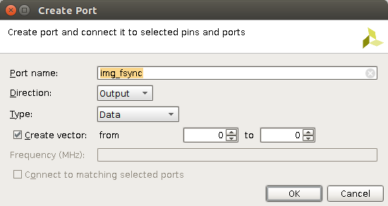
In this example, because the wire of interest is a bus (of size 1), I matched it. Then the top-level block diagram exposes the wires of interest like this:

Since I just modified the system's interface, I have to regenerate the wrapper Verilog file: system_wrapper.v, by right-clicking on the system.bd node in Vivado Sources view --> Create HDL Wrapper --> Let Vivado manage wrapper and auto-update (since I have no reason to modify the wrapper itself). But I ran into a problem generating the wrapper due to this error:
CRITICAL WARNING: [BD 41-1336] One or more IPs are locked in this design 'system.bd'. Please run report_ip_status for more details and recommendations on how to fix this issue.
I suspected that my repacking of img_stream caused this problem, so I ran the following TCL command in Vivado TCL console and confirmed my suspicion:
foreach x [get_ips] {puts $x; puts [get_property IS_LOCKED $x]}
I worked around the problem by deleting img_stream IP and adding it back again (and reconnecting the wires of course). A BETTER alternative is to upgrade the IP within the top level project: menu --> Tools --> Report --> IP status --> select the modified IP and click "Upgrade". I could see that Vivado automatically upgrades the version number whenever I make a change.
INFO: [IP_Flow 19-3422] Upgraded system_img_stream_0_1 (img_stream_v1.0 1.0) from revision 3 to revision 4
INFO: [IP_Flow 19-3471] Wrote upgrade log to '/mnt/work/zynq/vivado/adv7511_zed.srcs/sources_1/bd/system/ip/system_img_stream_0_1/system_img_stream_0_1.upgrade_log'.
Wrote : </mnt/work/zynq/vivado/adv7511_zed.srcs/sources_1/bd/system/system.bd>
The top level Verilog file then brings out the wires from the system wrapper.
module system_top (
output MT9P031_CLK,
output[3:0] img_tdata,
output img_tlast, img_tready, img_tvalid, img_fsync,
...
wire[31:0] img_tdata_wire;
//Look at the even and odd pixel LSB
assign img_tdata = {img_tdata_wire[17:16], img_tdata_wire[1:0]};
system_wrapper i_system_wrapper (
...
.img_tdata(img_tdata_wire),
.img_tlast(img_tlast),
.img_tready(img_tready),
.img_tuser({img_fsync}),
.img_tvalid(img_tvalid),
...
Finally, the pins are constrained in the XDC file. For serious FPGA development, the FMC breakout board FMC-105-debug is essential, to get at as many internal wires as possible. On the FMC-105-debug, many of the pins are on the VADJ I/O bank (either 1.8 V or 2.5 V). There is no point in exposing the 100 Mhz FLCK_CLK0 to logic analyzer, because my Saleae Logic Pro 16's sampling rate is only 100 MHz. But the 8 wires connected to the system wrapper should easily be visible on VADJ I/O, say at FMC-105-debug J1 (schematic shown in Xilinx document XTP078), pins FMC_LA{10,11,12,13}_P/N. So I can place them all in Zynq bank 34 (VADJ):
- img_tdata[3]: J1.2, FMC_LA10_P, Zynq pin R19
- img_tdata[2]: J1.4, FMC_LA10_N, Zynq pin T19
- img_tdata[1]: J1.6, FMC_LA11_P, Zynq pin N17
- img_tdata[0]: J1.8, FMC_LA11_N, Zynq pin N18
- img_tvalid: J1.10, FMC_LA12_P, Zynq pin P20
- img_fsync: J1.12, FMC_LA12_N, Zynq pin P21
- img_tlast: J1.14, FMC_LA13_P, Zynq pin L17
- img_tready: J1.16, FMC_LA13_N, Zynq pin M17
The constraint entries then work out to this:
set_property -dict {PACKAGE_PIN R19 IOSTANDARD LVCMOS18} [get_ports img_tdata[3]];#FMC_LA10_P --> FMC-105 J1.2
set_property -dict {PACKAGE_PIN T19 IOSTANDARD LVCMOS18} [get_ports img_tdata[2]];#FMC_LA10_N --> FMC-105 J1.4
set_property -dict {PACKAGE_PIN N17 IOSTANDARD LVCMOS18} [get_ports img_tdata[1]];#FMC_LA11_P --> FMC-105 J1.6
set_property -dict {PACKAGE_PIN N18 IOSTANDARD LVCMOS18} [get_ports img_tdata[0]];#FMC_LA11_N --> FMC-105 J1.8
set_property -dict {PACKAGE_PIN P20 IOSTANDARD LVCMOS18} [get_ports img_tvalid]; #FMC_LA12_P --> FMC-105 J1.10
set_property -dict {PACKAGE_PIN P21 IOSTANDARD LVCMOS18} [get_ports img_fsync]; #FMC_LA12_N --> FMC-105 J1.12
set_property -dict {PACKAGE_PIN L17 IOSTANDARD LVCMOS18} [get_ports img_tlast]; #FMC_LA13_P --> FMC-105 J1.14
set_property -dict {PACKAGE_PIN M17 IOSTANDARD LVCMOS18} [get_ports img_tready]; #FMC_LA13_N --> FMC-105 J1.16
After generating bitstream for this modified HW, I export the HW and the bitstream to the SDK and step into the FW land.
[Optional] learn from the standalone BSP code
This is the note I took while trying to understand the Xilinx VDMA IP. You may skip to the next section, where I write a bare metal C code to DMA 1 frame.The standalone BSP peripheral list in system.mss is also updated, as shown below

*|<----------------- FRAME_HORIZONTAL_LEN ---------------------->|
* --------------------------------------------------------------------
*| | ^
*| | |
*| |<-SUBFRAME_HORIZONTAL_SIZE ->| | FRAME_
*| ----------------------------------- | VERTICAL_
*| |/////////////////////////////| ^ | LEN
*| |/////////////////////////////| | | |
*| |/////////////////////////////| | | |
*| |/////////////////////////////| SUBFRAME_ | |
*| |/////////////////////////////| VERTICAL_ | |
*| |/////////////////////////////| SIZE | |
*| |/////////////////////////////| | | |
*| |/////////////////////////////| v | |
*| ---------------------------------- | |
*| | v
*--------------------------------------------------------------------
The vdma is responsible for transferring the SUBframe to DRAM. If the subframe starts 5 rows and 32 columns from the upper left corner of the frame, the subframe's start is defined as
#define SUBFRAME_START_OFFSET (FRAME_HORIZONTAL_LEN * 5 + 32)
Starting the transfer is a 2 step process:
* --------------------------------------------------------------------
*| | ^
*| | |
*| |<-SUBFRAME_HORIZONTAL_SIZE ->| | FRAME_
*| ----------------------------------- | VERTICAL_
*| |/////////////////////////////| ^ | LEN
*| |/////////////////////////////| | | |
*| |/////////////////////////////| | | |
*| |/////////////////////////////| SUBFRAME_ | |
*| |/////////////////////////////| VERTICAL_ | |
*| |/////////////////////////////| SIZE | |
*| |/////////////////////////////| | | |
*| |/////////////////////////////| v | |
*| ---------------------------------- | |
*| | v
*--------------------------------------------------------------------
The vdma is responsible for transferring the SUBframe to DRAM. If the subframe starts 5 rows and 32 columns from the upper left corner of the frame, the subframe's start is defined as
#define SUBFRAME_START_OFFSET (FRAME_HORIZONTAL_LEN * 5 + 32)
In XAxiVdma_CfgInitialize(), the MM2S and S2MM channels within XAxiVdma structure are initialized separately. Each channel can have up to MAX_FRAMESTORE number of BDs (buffer descriptors). Because the DMA HW will read BD, it has to be word aligned:
typedef struct {
...
XAxiVdma_Bd BDs[XAXIVDMA_MAX_FRAMESTORE] __attribute__((__aligned__(32)));
/*Statically allocated BDs */
u32 DbgFeatureFlags; /* Debug Parameter Flags */
}XAxiVdma_Channel;
As shown in Xilinx document PG020 AXI VDMA Table 2-3, MM2S control registers are at the base address of the VDMA memory map, while the S2MM control registers are at offset 0x30 from the VDMA memory map base. For example, line buffer threshold (not the size of the buffer itself) is programmable through one of the registers in this range. MM2S frame registers begin again at offset 0x50, and S2MM frame registers begin again at offset 0xA0.
The example code then sets up "NumFrames" number of BD ring--forming the ring happens at the last BD. Each buffer descriptor's pointer is a PHYSICAL address (using XAXIVDMA_VIRT_TO_PHYS macro).
The channel is then soft reset (pending command/transfers are flushed/completed) by writing 0x4 to the control register--consistent with PG020 AXI VDMA Figure 2-2. Because the reset is not hard, the SW polls the same bit to ensure that reset has completed.
In case you want to use a smaller number of frame stores than the VDMA instance was configured for (why would you? Besides, recall that my first vdma instance has only 1 frame store), the frame store register is set next--but the channel must not be running (the SR halted bit is set or the CR running bit is deasserted) for the frame number change to be allowable.
The example then writes the frame and delay timer count. To recap, both of these counts control VDMA interrupt into the CPU:
- Normally, the HW will interrupt the CPU when the successful frames transferred count reaches the frame count set in the CR register. For monitoring the status of multi-frame transfer, periodically read PARK_PTR_REG (which is RO).
- But if the transfer stalls, the HW will also interrupt the CPU if delay count != 0.
A channel is configured with following possibilities through the configuration registers:
- Circular_Park = 1: engine cycles through the frame buffers; irrelevant if NUM_FSTORE = 1 (my case). If parking, the frame to park on must be written to the FRAMEPARK register (offset 0x28).
- Genlock synchronization and source: irrelevant for genlock master
- Frame count enable: stop the engine after desired number of frame transfer. This goes together with FrmCnt_IrqEn and DlyCnt_IrqEn explained in the above paragraph.
- In SG mode, a frame's vertical size, horizontal size, stride, and frame delay are written to the BDs. In the generated example, the ROI is 100x100, and stride is 1920. Frame delay is relevant in the genlock case, where the genlock slave trails the genlock master by the specified number of frames. But in the register direct mode (the usual case for Xilinx supplied examples), only the ROI horizontal size, the stride, and the frame delay are written to the HW.
- The DRAM address for each frame (frame store in VDMA terminology) are written to the {MM2S|S2MM}_START_ADDRESS{1~32}. To save resources, this HW uses register banking to overlap the address of the frames 17~32 on top of the 1~16. In case N_FRAME_STORE <= 16, I can ignore this banking behavior. Each frame store is big enough to store the complete frame (rather than just the ROI)--which is 1920x1080 in this example. But for some reason, ADDRESS1 starts at SUBFRAME_OFFSET defined above from the beginning of the DRAM area set aside for DMA, which is hard coded at 0x2000000 in this example. So it is important to remember that a frame in VDMA terminology is big enough to cover every pixel, including the blanking area, but the address starts at the beginning of the ROI. I cannot think of a reason why the frame's horizontal size would be different than the stride size, both of which are in bytes--except for horizontal blank > 0.
The interrupt priority and trigger (same as the CPU target) is configured through the GUI distributor registers, according to the explanations in Zynq TRM register explanation for GIC_PRIORITY0 and GIC_SPI_TARGET. For the example, the BSP level interrupt handler clears the pending interrupt by writing to the status register, while the application level interrupt handler simply checks the interrupt status for ether the frame count reaching 0, or error bit.
- If the channel is idle:
- For SG case, the 1st BD's physical address is written to {MM2S|S2MM}_CURDESC register (offset 0x8).
- Assert the run bit in the control register
- By now, the channel should be running (DMA engine has started), so that we can:
- For SG case, the channel's tail BD physical address is written to the {MM2S|S2MM}_TDESC register.
- else (direct register mode), write number of rows in ROI to VSIZE register.
Bare metal code for 1-at-a-time, non scatter-gather frame DMA
In XSDK, the updated HW definition now includes the address map for for img_stream and img_vdma: 0x43C0000 and 0x43010000, respectively.
To write a compact bare metal code, segment the properties of the VDMA into invariant (for my application) and those that will change with each capture:
- Same for all captures
- DMACR
- IRQ delay count = 0 (default). I will instead use a private timer (which already paces the system tick in my bare metal code).
- IRQ frame count = 1 (default). I will transfer 1 frame at a time.
- Err_IrqEn = 1. Enable error interrupt. The errors (in status register) I care about are:
- DMA decode error (1 << 6)
- DMA slave error (1 << 5)
- DMA internal error (1 << 4)
- FrmCnt_IrqEn = 1. All frames (1) transferred interrupt.
- FsyncSrcSelect = 2. s_axis_s2mm_tuser[0]--although irrelevant for now, since I disabled FSYNC feature.
- FrameCntEn = 1. VDMA engine stops on its own after desired number of transfers.
- THRESHOLD: high water mark; 75% a good heuristic
- FRMSTORE: left at default (IP configuration parameter)
- FRMDLY: left at 0 (default), since I do not use genlock
- Start address: the 1st start address is fixed in my static memory map (divided between Linux, the uncached region (big enough for 1 full frame) for this DMA, and the bare metal code.
- Changes across capture, or within the capture
- DMACR
- RS: when capturing a frame, start the engine with this bit.
- RESET: to recover from error
- HSIZE: ROI line size in byte changes for each capture
- VSIZE: ROI height changes for each capture
- STRIDE (in FRMDLY_STRIDE register): number of bytes of each line changes for each capture even if horizontal blanking = 0, because the ROI changes.
With this background, let's dive into the C++ implementation.
#define IMG_STREAM(offset) (*(volatile uint32_t*)(0x43C00000 | offset))
#define IMG_STREAM_CTRL IMG_STREAM(0)
uint32_t status = IMG_STREAM_CTRL;//Confirm the img_stream version
#define IMG_STREAM_VER_EXPECTED 0x6
Q_ALLEGE(((status >> 1) & 0x7F) == IMG_STREAM_VER_EXPECTED);
Assert the custom IP version
Recall that I exposed my custom IP (img_stream) version number to a read-only register bit (offset 0). This is how to assert against expected version, using the QP framework's Q_ALLEGE macro, which works similar as the well-known assert macro:#define IMG_STREAM(offset) (*(volatile uint32_t*)(0x43C00000 | offset))
#define IMG_STREAM_CTRL IMG_STREAM(0)
uint32_t status = IMG_STREAM_CTRL;//Confirm the img_stream version
#define IMG_STREAM_VER_EXPECTED 0x6
Q_ALLEGE(((status >> 1) & 0x7F) == IMG_STREAM_VER_EXPECTED);
Configure VDMA interrupt
As I explored in a previous blog entry, bare metal Zynq interrupt setup in AMP environemnt involves the following elements:
- Enable interrupt in the Zynq SCU GIC (generalized interrupt controller HW)'s distributor.
- Configure the interrupt target and [optionally] priority
The code for the 1st step requires that we know the desired interrupt number--which I discussed above. Therefore, the code is:
enum InterruptId {
...
INT_ID_PL12 = 88,//56 + 32, spi_status1[24]
};
#define XPAR_PS7_SCUGIC_0_DIST_BASEADDR 0xF8F01000
#define ZYNQ_INTERRUPT_ENABLE(group) *(volatile uint32_t*)\
(XPAR_PS7_SCUGIC_0_DIST_BASEADDR + 0x100 + 4*group)
ZYNQ_INTERRUPT_ENABLE(2) = //See ICDISER2: for intID 64~95 (shared)
1 << (INT_ID_PL12 % 32);
Writing to the target register is complicated because a single 32-bit register holds the target of 4 different interrupt numbers; I have to be careful about not disturbing other interrupts.
#define ZYNQ_INTERRUPT_TARGET(group) *(volatile uint32_t*)\
(XPAR_PS7_SCUGIC_0_DIST_BASEADDR + 0x800 + 4*(group))
#define ZYNQ_INTERRUPT_TARGET_MASK_SHIFT(intID) (((intID) % 4) * 8)
//2'b10: target CPU1
#define ZYNQ_INTERRUPT_TARGET_MASK_CPU1(intID) \
(2 << ZYNQ_INTERRUPT_TARGET_MASK_SHIFT(intID))
#define ZYNQ_INTERRUPT_TARGET_MASK_CPU01(intID) \
(3 << ZYNQ_INTERRUPT_TARGET_MASK_SHIFT(intID))
#define ZYNQ_INTERRUPT_TARGET_CPU1(intID) \
ZYNQ_INTERRUPT_TARGET((intID)/4) = \
ZYNQ_INTERRUPT_TARGET_MASK_CPU1(intID) | \
(~ZYNQ_INTERRUPT_TARGET_MASK_CPU01(intID) & \
ZYNQ_INTERRUPT_TARGET((intID)/4))
ZYNQ_INTERRUPT_TARGET_CPU1(INT_ID_PL12);
What would happen if I just left the target register at default value (target both CPUs)? Linux would receive the interrupt when VDMA asserts either an error or completion, and log a kernel error (I tried this already).
VMDA interrupt ISR
At minimum, the ISR must acknowledge the interrupt. Since I only use the interrupt for detecting an error or completion of a transfer, I choose to reset the VDMA HW--it keeps the SW simpler and arguably more robust.
#define IMG_VDMA(offset) (*(volatile uint32_t*)(0x43010000 | offset))
#define IMG_VDMA_WR_CTRL IMG_VDMA(0x30) //PG020 Table 2-14
#define IMG_VDMA_CTRL_RUNNING (1 << 0)
#define IMG_VDMA_CTRL_RESET (1 << 2)
#define IMG_VDMA_CTRL_RESTART IMG_VDMA_CTRL_RESET | IMG_VDMA_CTRL_RUNNING
#define IMG_VDMA_CTRL_COUNT_FRAME (1 << 4)
#define IMG_VDMA_STATUS_ERR (1<<14)//Err_Irq_En
#define IMG_VDMA_STATUS_TIMEOUT (1<<13)//DlyCnt_IrqEn
#define IMG_VDMA_STATUS_DONE (1<<12)//FrmCnt_IrqEn
#define IMG_VDMA_STATUS_INTERRUPT \
(IMG_VDMA_STATUS_ERR | IMG_VDMA_STATUS_TIMEOUT | IMG_VDMA_STATUS_DONE)
#define IMG_VDMA_CTRL_TUSER (2 << 5)
#define IMG_VDMA_N_FRAME 1
#define IMG_VDMA_CTRL_CONFIG ((IMG_VDMA_N_FRAME << 16) | IMG_VDMA_CTRL_TUSER \
| IMG_VDMA_STATUS_INTERRUPT | IMG_VDMA_CTRL_COUNT_FRAME)
#define IMG_VDMA_RESET() IMG_VDMA_WR_CTRL = \
(IMG_VDMA_CTRL_CONFIG | IMG_VDMA_CTRL_RESTART)
#define IMG_VDMA_WR_STATUS IMG_VDMA(0x34) //PG020 Table 2-15
uint32_t status = IMG_VDMA_WR_STATUS;
IMG_VDMA_WR_STATUS = status;//acknowledge the interrupt
//Just reset the whole HW, instead of only turning off the interrupts
IMG_VDMA_RESET();
Finally, I am ready to actually "do the deed".
Setting up a VDMA write before starting the image "capture"
With all the macros introduced above, the multi-phased VDMA setup can begin--with the HW reset of course.
IMG_VDMA_RESET();
IMG_STREAM_CTRL = 0;//stop the img_stream
The reset make take some time, so I set a timer (not shown here) and check later:
status = IMG_STREAM_CTRL;
if(status & 1) {//img_stream should be idle
go to error state
}
//img_stream IP has to know the max column number and row number
IMG_STREAM_SIZE = (uint32_t)((me->col_size+1)/2 - 1) << 16
| me->row_size;
status = IMG_VDMA_WR_CTRL;
//If I got an I2C success, many clock cycles has passed, so
//that it would be valid to check that reset has completed
if(status & IMG_VDMA_CTRL_RESET) {//Reset still in progress?
go to error state
}
After resetting, I start the DMA engine:
IMG_VDMA_WR_CTRL = IMG_VDMA_CTRL_CONFIG | IMG_VDMA_CTRL_RUNNING;
And after waiting for some time again, I configure the frame specific registers:
status = IMG_VDMA_WR_CTRL; //img_vdma should be running by now
if(!(status & IMG_VDMA_CTRL_RUNNING)) {
go to error state
}
#define IMG_VDMA_WR_ADDR1 IMG_VDMA(0xAC) //PG020 Table 2-28
IMG_VDMA_WR_ADDR1 = me->frame_addr;
uint16_t row_bytes = (me->col_size+1)*2;//because each pixel is 16-bit
#define IMG_VDMA_WR_LOCK_DELAY_STRIDE IMG_VDMA(0xA8) //PG020 Table 2-27
IMG_VDMA_WR_LOCK_DELAY_STRIDE = row_bytes;//Should stride = row?
#define IMG_VDMA_WR_ROW_BYTES IMG_VDMA(0xA4) //PG020 Table 2-26
IMG_VDMA_WR_ROW_BYTES = row_bytes;//HSIZE
#define IMG_VDMA_WR_HWM IMG_VDMA(0x4C)//threshold
IMG_VDMA_WR_HWM = 512 >> 1;//Set at half of line buffer bytes
#define IMG_VDMA_WR_VSIZE IMG_VDMA(0xA0) //PG020 Table 2-21
IMG_VDMA_WR_VSIZE = me->row_size + 1;
At the point, the VDMA is waiting for the pixels to come pouring in, which I trigger by hitting the img_stream's capture_cmd bit:
//Xilinx recommendation: clear interrupts before starting
IMG_VDMA_WR_STATUS = IMG_VDMA_WR_STATUS;
IMG_STREAM_CTRL = 1;//start img_stream
There are 3 ways this transfer can finish:
- VDMA error interrupt
- VDMA done interrupt
- The timeout I armed (not shown here) expires.
For the 1st 2 cases, the ISR can signal the main thread, and I can check the status register:
#define IMG_VDMA_KNOWN_ERRORS ((3 << 9) | (7 << 4))
if(status & IMG_VDMA_KNOWN_ERRORS) {
go to error state ...
} else {
wait for another capture command...
}
On success (the 2nd case above), Linux can read the content of the image sitting at the frame address known apriori.
Qt and Linux code to read DMAed frame
Similar to how I restricted Linux to use only a part of the entire DRAM in a previous blog entry, I whittled down the DRAM allotted to Linux even more with the "mem=500M" kernel parameter, leaving me 11 MB (the DRAM is 512 MB, but I use the last 1 MB for the bare metal real-time code I just presented above). In that previous blog entry, I also explored using mmap on the /dev/mem file to read/write OCM (on-chip-memory). I use the same technique to read the portion of the DRAM that the VDMA just wrote into, by creating another mmap into /dev/mem--but with a different address of course.
#define DRAM_SIZE (512 * 1024 * 1024)
#define FW_SIZE ( 1 * 1024 * 1024)
#define IMG_DMA_SIZE (11 * 1024 * 1024) //5 Mpixel * 2 byte/pixel = 10 MB
#define DMA_LOC (DRAM_SIZE - FW_SIZE - IMG_DMA_SIZE)
l_memf = open("/dev/mem"
, O_RDWR /*| O_SYNC*/); //do I want cacheing?
BSP_dma = (char*)mmap(NULL, IMG_DMA_SIZE, PROT_READ | PROT_WRITE,
MAP_SHARED /*| MAP_LOCKED*/,
l_memf, DMA_LOC);
qDebug("BSP_dma @ %p", BSP_dma);
Then I can look into this uncached (because mmap creates an uncached virtual memory region) any time:
QString msg = QString("img_vdma status 0x%1; DMA content:")
.arg(evt->u32[1], 8, 16, QChar('0'));
for(uint8_t i=0; i<32; ++i) {
msg += QString(" %1,")
.arg(*((uint16_t*)BSP_dma + i), 4, 16, QChar('0'));
}
gui->statusBar->showMessage(msg);
#define DRAM_SIZE (512 * 1024 * 1024)
#define FW_SIZE ( 1 * 1024 * 1024)
#define IMG_DMA_SIZE (11 * 1024 * 1024) //5 Mpixel * 2 byte/pixel = 10 MB
#define DMA_LOC (DRAM_SIZE - FW_SIZE - IMG_DMA_SIZE)
l_memf = open("/dev/mem"
, O_RDWR /*| O_SYNC*/); //do I want cacheing?
MAP_SHARED /*| MAP_LOCKED*/,
l_memf, DMA_LOC);
qDebug("BSP_dma @ %p", BSP_dma);
QString msg = QString("img_vdma status 0x%1; DMA content:")
.arg(evt->u32[1], 8, 16, QChar('0'));
for(uint8_t i=0; i<32; ++i) {
msg += QString(" %1,")
.arg(*((uint16_t*)BSP_dma + i), 4, 16, QChar('0'));
}
gui->statusBar->showMessage(msg);
On my logic analyzer, it took just over 50 ms to write slightly less than 10 MB into the DRAM, so that the DMA bandwidth was roughly 200 MB/s. Considering that the FPGA logic clock (FCLK_CLK0) is only running at 100 MHz in this HW design, and it can potentially be increased to 600 MHz, there is plenty of headroom for speedup should I need it (I don't for now). What matters more is correctness; recall that I wrote {row, col} from the img_stream IP. What I see in my Qt GUI's status bar is flipped for some reason:
0000 0000 0001 0000 0002 0000 0003 0000 ...
Rendering the image in a Qt GUI
As explained in a previous blog entry, I have been exposing the low level HW I create on my Zedboard through the Qt widgets GUI. Once the bare metal code indicates to the Linux userspace application about a successful capture (see my previous blog entries--like this and this--for how I do this), the Qt GUI can render the image that is still sitting in the DMA area--by reading directly from it. Of course, even that last reading would be unnecessary if the vdma DMAed directly to a GPU, but the only chink in the Zedboard's armor is the lack of on-chip GPU. Ultrascale processor now has a Mali GPU, but it will take at least year for the Xilinx community to ramp up to the Ultrascale. Meanwhlie, a delay of a couple of seconds to render approximately 5 M pixels on CPU0 is the best I can do.
While QLabel widget's ability to render all kinds of image formats is wonderful, it does NOT support monochrome pixel format, so I make do with the RGB16 format, which interprets each pixel of packed 16-bit unsigned matrix as consisting of 5 bits of R, 6 bits of G, and 5 bits of B. The key is to form a QImage on the stack that points to the raw DMA data, like this:
QImage img((uchar*)BSP_dma, width, height, QImage::Format_RGB16);
where BSP_dma is the mmapped address obtained above. If I transform the QImage into a QPixmap (TODO: investigate whether it's faster to load the data directly to QPixmap), then I QLabel can take care of the rest:
gui->sensorForm->lblImg->setPixmap(QPixmap::fromImage(img));
where sensofForm is the UI form I created in the Qt Creator, and lblImg is the QLabel placed in that form. Note that the above code should be called only from the Qt GUI thread. This is what the test pattern looks like when I execute the above code:
 The gradual transition to green is because as the row number increases, the "green" in RGB16 format becomes more prominent.
While QLabel widget's ability to render all kinds of image formats is wonderful, it does NOT support monochrome pixel format, so I make do with the RGB16 format, which interprets each pixel of packed 16-bit unsigned matrix as consisting of 5 bits of R, 6 bits of G, and 5 bits of B. The key is to form a QImage on the stack that points to the raw DMA data, like this:
QImage img((uchar*)BSP_dma, width, height, QImage::Format_RGB16);
where BSP_dma is the mmapped address obtained above. If I transform the QImage into a QPixmap (TODO: investigate whether it's faster to load the data directly to QPixmap), then I QLabel can take care of the rest:
gui->sensorForm->lblImg->setPixmap(QPixmap::fromImage(img));
where sensofForm is the UI form I created in the Qt Creator, and lblImg is the QLabel placed in that form. Note that the above code should be called only from the Qt GUI thread. This is what the test pattern looks like when I execute the above code:
Saving the raw data as a TIFF file
In biotech/biomedical field, 16-bit monochrome images is frequently used as the source image for complex image processing. There are many great tools out there--many of them free and open source--to interact with TIFF file. Since QImage does NOT support this format, I fall back to yet another great free and open source library to do the heavy lifting: opencv (specifically, the highgui module). Given a raw pointer to the image, this code creates a new TIFF file:
cv::Mat mat(height, width, CV_16U, BSP_dma);
QString fname = QDateTime().toString("MMddhhmmss") +
QString("_%2x%3.tiff").arg(width).arg(height);
cv::imwrite(fname.toLatin1().data(), mat);
The created file is 13 MB, suggesting an uncompressed TIFF format:
$ ls -lh
13M Jun 6 19:29 _2592x1944.tiff
But tiffinfo tools says an LZW compression was used!?
# tiffinfo _2592x1944.tiff
TIFF Directory at offset 0xc4b192 (12890514)
Image Width: 2592 Image Length: 1944
Bits/Sample: 16
Compression Scheme: LZW
Photometric Interpretation: min-is-black
Samples/Pixel: 1
Rows/Strip: 1
Planar Configuration: single image plane
Predictor: horizontal differencing 2 (0x2)
TIFF Directory at offset 0xc4b192 (12890514)
Image Width: 2592 Image Length: 1944
Bits/Sample: 16
Compression Scheme: LZW
Photometric Interpretation: min-is-black
Samples/Pixel: 1
Rows/Strip: 1
Planar Configuration: single image plane
Predictor: horizontal differencing 2 (0x2)
TODO: a custom QWidget that paints the 16-bit monochrome
It is customary to indicate saturated pixel (0xFFFF in case of 16-bit pixel) with pure red, for debugging purpose.
Appendix: ARM PL330 DMA HW
Fundamentally, all DMA on the system is mediated by the DMA controller. In Zynq 7020 (on Zedboard) case, ARM's PL 330 IP core. I never looked into the details of a DMA controller, but I read the PL 330 manual, and discovered that the DMA engine executes DMA instruction set (called microcode, which is different than the CPU instruction set) using its own RAM, FIFO, and cache. Therefore, a DMA controller is more like a simple (and dedicated) microcontroller than a dumb IO peripheral (like I2C). DMA controller is a shared system resource--not just between the multiple CPU cores, but all HW in the system that can read/write--so must be concurrency protected.Bringing up a new CPU is a difficult work, so bringing up a DMA controller that works with the main CPU is probably also difficult. Fortunately, Xilinx reduced the pain by offering a higher layer IP blocks that mediate transactions with memory and the DMA controller.
Appendix: Xilinx DMA IP cores
Xilinx gives away the AXI DMA block, and supplies Linux device drivers (<kernel>/drivers/dma/xilinx_dma.c):- axi_cdma IP core (central memory DMA) is for memory <--> memory DMA (ds792_axi_cdma.pdf).
- axi_dma IP core is for memory <--> peripheral DMA (pg021_axi_dma.pdf).
- axi_vdma core (video DMA): pg020_axi_vdma has video frame sync feature
Of these, the AXI VDMA core is best suited for moving frames around, because it is both frame, line, and even stride (relevant when ROI size is less than the full frame size) aware.
A lower performance but less FPGA-resource-intensive mode can be enabled by excluding the Scatter Gather engine. In this mode transfers are commanded by setting a Source Address (for MM2S) or Destination Address (For S2MM) and then specifying a byte count in a length register.
To get the best possible throughput for AXI VDMA instances, the maximum burst length is set to 16. In addition, the master interfaces have a read and write issuance of 8 and a read and write FIFO depth of 512 to maximize throughput. The line buffers inside the AXI VDMA for the read and write sides are set to 4K deep and the store and forward feature of the AXI VDMA are enabled on both channels to improve system performance and reduce the risk of system throttling. Q: why are both the line buffer and store-and-forward necesary?
axi_vdma IP
This IP is frame boundary aware, and can do uninterrupted transfers to a circular buffer of frames (stored in RAM of course). If Nframe = 1 (the default), the transfer is 1 at a time.
Frame delay: In frame sync mode (vs. free run mode), a pin s2mm_fsync can externally trigger the start of the transfer. Q: but where would the vdma IP store the pixels while waiting for the trigger?
Frame sync: since the sensor pixel collector IP (the one that picks up the pixel bus and performs horizontal binning if necessary) runs based on the sensor's PIXCLK, free run mode cannot be used.
Flush on frame sync: if FSYNC=1, the logic can restart transfer at the beginning of a new frame even after a DMA error detection.
DDR becomes unavailable during refresh, so line buffer is necessary. Using the same FIFO used for the line buffer feature, the store-and-forward feature prevents the IP from issuing read/write to RAM unless there is enough room/data to complete the read/write. Store-and-forward buffer is the recommended guard against deadlock on a single-ported RAM in a loop-back test.
The following debugging features may be useful:
- C_S2MM_SOF_ENABLE: asserted on the 1st pixel of first line for each frame.
- C_S2MM_LINEBUFFER_THRESH (default 4) almost full flag asserts when the line buffer gets near full.
- s_axis_s2mm_tready asserts after fsync_out asserts, indicating that the IP is ready to accept data. It deasserts when all expected data is received.
In register direct mode (vs. scatter-gather mode), the processor can program the start address and video parameters. For a single ROI (region of interest) data, the register direct mode avoids the complications arising from having to read the SG buffer descriptors from the memory. The registers are memory mapped; some important registers are:
- DMACR/DMASR [only for register direct mode]: DMA control and status
- interrupt enable
- frame/delay count
- IP is running when DMACR[RS] = 1 and DMASR[Halted] = 0.
- MM2S_VSIZE/S2MM_VSIZE register: In Register Direct Mode (C_INCLUDE_SG = 0) indicates vertical size in lines of the video data to transfer. There are vsize number of packets that are hsize bytes long transmitted for each frame. Writing to this register starts the VDMA transfers on MM2S Channel. Valid HSIZE, STRIDE, and Start Addresses must be set prior to writing MM2S_VSIZE. On S2MM, HSIZE and VSIZE will be set AFTER s2mm_prmtr_update.
- S2MM_FRMDELAY_STRIDE: In Register Direct Mode (C_INCLUDE_SG = 0) indicates the number of address bytes between the first pixels of each video line. Must be > S2MM_HSIZE.
- S2MM_START_ADDRESS[1~N]: There are C_NUM_FSTORES start addresses for each channel. START_ADDRESS[0] offset is 0xAC, and goes up by 4 bytes consecutively for each subsequent START_ADDRESS. On error, the frame store pointer is updated with the frame reference of the errored frame
AXI buses
Initialization, status, and management registers in the AXI VDMA core are accessed through the slower AXI4-Lite slave interface (AXI ACP). Data flows through higher performance AXI stream buses (AXI_HP).[optional] Video timing detector IP
If I did NOT know apriori the frame format, this IP might be helpful: the video timing generator/detector block and AXI Lite interface of this core work on a
single clock domain, that is, the video clock. For detailed information on the complete feature set and a functional description of AXI VTC IP, refer to PG016, LogiCORE IP Video Timing Controller Product GuideAppendix: Zedboard reference HW design
In the kernel I've been using since Qt5 on Zedboard example, DMA related kernel configs were already turned on, as you can see in my defconfig file:
CONFIG_DMADEVICES=y
CONFIG_XILINX_DMA=y
CONFIG_PL330_DMA=y
CONFIG_DMA_AXI_DMAC=y
In the HW design (Vivado), the axi_hdmi_dma IP block handles moving video data from DRAM to FPGA, as you can see in this screenshot, where the high bandwidth M_AXI_MM2S data--highlighted yellow in the screenshot--comes over the AXI_HP bus (direct connection to the PS7's AXI_HP0 port--well, through the axi_hdmi_interconnect):

Note that this IP only has the master to slave ports. mms2_fsync, mm2s_tkeep, mms2_tlast, mm2s_tlready, mm2s_tvalid--used for throttling--all feed the axi_hdmi core (which then connects to the ADI ADV7511 chip). mms2s_tdata, the pixel data originates from the processor's S_AXI_HP0 port, and is sent to the HDMI vdma IP (above) through the AXI HDMI interconnect--even though the data ultimately comes from DDR RAM, as shown below:
 The HDMI interconnect has 1 master-slave port pairs because it was configured with just 1 interface each in the IP configurator, as shown below:

On the Zynq side, S_AXI_HP0, which is an instance of the AFI ports having read/write FIFOs and 2 dedicated memory ports on DDR (and a path to OCM--which is irrelevant for most cases) as shown in the following schematic taken from the Zynq TRM (in the Interconnect chapter):
 Note that there are only 2 DDR controller master ports (logic, really) for the 4 AXI_HP ports (AFI), and that HP0 and HP1 share the same DDR controller master ports (M0). Since we HP0 is already being used, I should use HP1 to avoid memory contention that the DDRC might see if I use either HP2 or HP3.
The HP0 port instance was configured in the Vivado PS7 configuration wizard as shown below:
 It is apparently allowed to access the entire DRAM on the Zedboard, as shown in the screenshot of the "Address Editor":

Since this HW is used for driving the HDMI display and I KNOW that the display currently works, the HW was necessarily described in DTS (zynq-zed-adv7511.dtsi):

On the Zynq side, S_AXI_HP0, which is an instance of the AFI ports having read/write FIFOs and 2 dedicated memory ports on DDR (and a path to OCM--which is irrelevant for most cases) as shown in the following schematic taken from the Zynq TRM (in the Interconnect chapter):

The HP0 port instance was configured in the Vivado PS7 configuration wizard as shown below:
Since this HW is used for driving the HDMI display and I KNOW that the display currently works, the HW was necessarily described in DTS (zynq-zed-adv7511.dtsi):
axi_hdmi@70e00000 {
compatible = "adi,axi-hdmi-tx-1.00.a";
reg = <0x70e00000 0x10000>;
encoder-slave = <&adv7511>;
dmas = <&axi_vdma_0 0>;
dma-names = "video";
clocks = <&hdmi_clock>;
};
compatible = "adi,axi-hdmi-tx-1.00.a";
reg = <0x70e00000 0x10000>;
encoder-slave = <&adv7511>;
dmas = <&axi_vdma_0 0>;
dma-names = "video";
clocks = <&hdmi_clock>;
};
The driver for the axi_hdmi is ADI kernel's <>/drivers/gpu/drm/adi_axi_hdmi/axi_hdmi_drv.c, written by Lars Clausen. But there is another DTS entry for the same IP axi_vdma, meant for the Xilinx VDMA driver <>/drivers/dma/xilinx_dma.c (or is it <>/drivers/staging/video/axivdma/xvdma.c?):
axi_vdma_0: axivdma@43000000 {
compatible = "xlnx,axi-vdma";
...
dma-channel@43000000 {
compatible = "xlnx,axi-vdma-mm2s-channel";
interrupts = <0 59 0x4>;
...
};
};
0x43000000 is the memory mapped register to control the HDMI DMA IP over AXI Lite interface shown above.
axi_vdma_0: axivdma@43000000 {
compatible = "xlnx,axi-vdma";
...
dma-channel@43000000 {
compatible = "xlnx,axi-vdma-mm2s-channel";
interrupts = <0 59 0x4>;
...
};
};
So my kernel already had these devices:
# ls /sys/devices/soc0/fpga-axi@0/
41600000.i2c fpga-axi@0:adv7511_hdmi_snd
43000000.axivdma fpga-axi@0:audio_clock
70e00000.axi_hdmi fpga-axi@0:zed_sound
75c00000.axi-spdif-tx modalias
77600000.axi-i2s power
79000000.axi-clkgen subsystem
0x43000000 is the memory mapped register to control the HDMI DMA IP over AXI Lite interface shown above.
Learning from the Xilinx Linux device driver source
During the device probe, the device driver hard codes the DMA_SLAVE and DMA_PRIVATE dma_device flags. What does this mean? The AXI VDMA device driver implements the following dma_device methods:
- xilinx_vdma_prep_slave_sg: irrelevant for direct register mode (simpler than scatter-gather)
- int (*device_control)(struct dma_chan *chan, enum dma_ctrl_cmd cmd, unsigned long arg): device_control: xilinx_vdma_device_control responds to the following DMA control commands:
- DMA_TERMINATE_ALL
- DMA_SLAVE_CONFIG
- Park (breaks the circularity of the frame) if vsize == -1
- interrupt coalescing and delay if hsize == -1
- device_issue_pending: xilinx_dma_issue_pending
- starts transfer
- device_alloc_chan_resources: xilinx_dma_alloc_chan_resources
- device_free_chan_resources: xilinx_dma_free_chan_resources
- enum dma_status (*device_tx_status)(...): xilinx_tx_status
A channel is a child node of DMA device, and has the following methods:
- void (*start_transfer)(struct xilinx_dma_chan *chan): xilinx_vdma_start_transfer
- If channel error pending, cannot start transfer
- dma_halt(chan)
- If scatter-gather, write the 1st descriptor to the register
- Write DMA configurtion register with the frame count, circular feature bits
- Write park frame register (offset 0x28)
- dma_start()
- If SG, write the last buffer descriptor, else write VSIZE register (offset 0xA0), counting from the base of the direct
- S2MM_VSIZE register description in Xilinx document PG020, table 2-25: "Writing to this register starts the VDMA transfers on S2MM channel".
- IRQ handler: dma_intr_handler
- printk errors if any error bit is set, and then halts the DMA channel
- Completion --> start another transfer
- Schedule tasklet, which will clean up the buffer descriptor
A channel exposes the following files to the debugfs:
- regs and nregs: human-readable register names and value pairs
- base: IO remapped view of the raw HW registers
I cannot use an individual device driver directly; the methods above are invoked through the DMA engine API described in (<>/Documentation/dmaengine.txt).
chan = dma_request_slave_channel(&pdev->dev, "video");
For Zynq (ARM architecture), the DTS case looks for "dma-names" DTS property to find the channel that was registered during the driver probe. A channel is given exclusively to the requesting client driver until the client calls dma_release_channel().
Using the Linux DMA engine from another driver
The Linux kernel DMA transaction goes through the following lifecycle:- Allocate a DMA slave channel
- Set DMA controller parameters
- Get a descriptor for the transaction
- Submit the transaction to the DMA engine's queue
- Start the transaction (or just add to the queue)
- Wait for the transaction's completion
Allocate DMA channel
A channel name should identify the DMA controller owning the channel through the name given in either DTS or ACPI, like this example:
For Zynq (ARM architecture), the DTS case looks for "dma-names" DTS property to find the channel that was registered during the driver probe. A channel is given exclusively to the requesting client driver until the client calls dma_release_channel().
Configure DMA controller
device_control() interface method is called--for the Xilinx VDMA driver, xilinx_vdma_device_control implements the interface, reading and writing the control register (either MM2S or S2MM).Transaction descriptor
Buffer descriptors are intimately coupled to scatter-gather DMA, which is indispensable for data generated from the many protocol stack such as TCP/IP. But for frame oriented data, only a simple transaction descriptor is necessary. dmaengine_prep_slave_single() is really converting a single buffer without a descriptor to use a descriptor; other functions are provided which allow other DMA modes including cyclic and interleaved modes.
static inline struct dma_async_tx_descriptor *dmaengine_prep_slave_single(
struct dma_chan *chan, dma_addr_t buf, size_t len,
enum dma_transfer_direction dir, unsigned long flags)
{
struct scatterlist sg;
sg_init_table(&sg, 1);
sg_dma_address(&sg) = buf;
sg_dma_len(&sg) = len;
return chan->device->device_prep_slave_sg(chan, &sg, 1,
dir, flags, NULL);
}
For axi_vdma HW, the following register writes happen in the implementation method xilinx_vdma_prep_slave_sg() after xilinx_dma_alloc_transfer (which sets the tx_submit method to xilinx_dma_tx_submit and allocates a DMA memory from a DMA pool--meaning: small buffer size):
- HSIZE
- FRAME_DELAY and STRIDE
- SRC_ADDRESS
Submit transaction to the queue
dmaengine_submit() will not start the DMA operation, it merely adds it to the pending queue, calling the tx_submit function pointer set in the previous step, and returns a cookie for use in subsequent functions. The HW actually does NOT care about the monotonically increasing cookie number (per channel variable).
Start DMA transfer
The transactions in the pending queue can be activated by calling the issue_pending API dma_async_issue_pending(struct dma_chan *chan), which will wind up calling the start_transfer interface method --> xilinx_vdma_start_transfer implementation described above.
On completion of each DMA operation (channel status register's XILINX_DMA_XR_IRQ_IOC_MASK bit--0x1000 is set), the next in queue is started and a tasklet triggered. The tasklet will then call the client driver completion callback routine for notification.
Cleanup
For the non-scatter-gather case, there is only one transfer active at a time, and there is no need to update the axi_vdma register for the SG buffer management. If ever the SG buffer is used, read the code in xilinx_dma_update_completed_cookie().